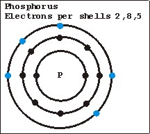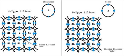
One dopant material used is phosphorus. Phosphorus has five electrons in its outer shell. What happens when a phosphorus atom joins the crystalline structure with silicon, is that one electron in its outer shell cannot pair with a silicon atom and is therefore left free. The free electron is a negative charge carrier and renders the silicon crystal electrically conductive and is called N-type silicon.

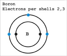
Boron is another dopant. This element has only three electrons in its outer shell. When this dopant is added during manufacturing there is a vacant space or hole where an “electron” can fit inside the silicon crystal lattice. The holes are considered positive charge carriers even though they do not contain a physical charge. The ability of silicon atom to accept another electron in its outer shell does make the hole (vacant space) appear to have a positive charge. The holes do render the silicon crystal conductive. The electron deficient silicon is called P-type silicon.

Its easy to imagine N-type material conducting electricity, using the free unbound electrons in the material. For P-type material it’s a little harder to understand. Imagine that electrons are jumping from one hole to another hole as they pass through the P-type material. To one looking at the electrons jumping it appears as if the holes in the silicon are moving in the opposite direction to the electron flow. The best analogy I’ve read that describes this process compares the holes tiny air bubbles moving through water.
While the N-type and P-type silicon materials conduct electricity, there are not as good as a conductor as copper. The conductivity of N and P type silicon lies between being conductors and insulators, hence they were given the name semiconductors.

